In 2002, Yuan Taur, a professor on the College of California, San Diego, had beforehand remained with Anuj Grover, a Doyen within the electrical engineering circle and a grasp’s diploma pupil in India, asking him to take his PhD below supervision. It was an enormous alternative – Glover is engaged on designing the gadgets. Nonetheless, he hesitated to search out out that there was little prospect of the job to pursue based mostly on this job. He declined the supply.
“If I needed to make the identical resolution at present, I might have jumped on the alternative,” Glover says from his workplace in Indraplast Info Institute (IIIT) Delhi.
In trendy technology-based items and companies economies, chips or semiconductors that management the move of electrical energy inside gadgets are most purposeful bedrock. From on a regular basis digital gadgets equivalent to fridges and vehicles to satellites and protection programs.
One main purpose he does so is that the federal government is pumped into electronics manufacturing, significantly semiconductors. Underneath the Indian semiconductor mission authorized by the Cupboard in 2021, there might be expenditures of 76,000 crores to ascertain India as a “international hub of digital manufacturing and design.” Over the previous two years, 10 giant amenities for the manufacture and meeting of chips have been authorized in six states, together with Gujarat, Punjab, Uttar Pradesh, Assam, Odisha and Andhra Pradesh.
The world is susceptible to operating chip and semiconductor designers, and Deloitte estimates there might be a spot between 1 million designers by 2030. India’s hope is a vital expertise pool. In response to trade estimates, one-fifth of all chip designers on this planet dwell right here. They work for multinational corporations like Nvidia and Intel, spreading throughout giant campuses. From 2021-22, there was a registration of Rs 57,000 for the graduate diploma course in electronics engineering. Nonetheless, a couple of points put the Indian chip design trade behind it.
Indian chip design edge
Foundry and chip meeting amenities, the place the silicon brains behind most trendy electronics are manufactured, are sponsored for as much as half the setup prices. In the meantime, different production-related incentive schemes are sponsored to telephones, PCs and different {hardware} meeting models by paying a portion of the values of all gadgets.
This technique has critics. Ragram Rajan, former India’s former Reserve Financial institution governor, has warned, alongside along with his frequent collaborator Rohit Lamba, that corporations aren’t retreating right into a market the place electronics is ripe for the manufacturing of electronics. Officers are affected by warnings and argue for the geopolitical significance of some management over world chip manufacturing.
Though India has a booming IT sector attributable to its concentrate on companies (the type proposed by Rajan), the federal government has argued that industrial bases with dents of digital gadgets aren’t viable, not after international chip crunches throughout the Covid-19 pandemic have introduced the provision chain to the knees. One space the place Rajan and the federal government are eye-catching is the significance of mental property and design, which India is already main. This development did not require the type of sopp that industrial initiatives are getting, critics say. Chip manufacturing might be costly and demanding when it comes to sources equivalent to ultra-pure gold, uninterrupted energy provide, and heavy equipment imported from abroad, however it’s only a PC or some take a look at gear in its design.
Semiconductors as city planning
Particular person ideas – the kind utilized in cellphones – barely cowl the tip of your finger. Some printed circuit boards with a number of chips soldered are additionally not that massive. Nonetheless, Professor IIIT-Delhi’s Glover feels that it must be in comparison with a a lot bigger one to know the world of chipmaking.
“Cities want city planners, architects, masons, carpenters and plumbers,” says Glover, mapping every of those roles to chip manufacturing equivalents. City Planners are semiconductor architects, with a mixture of administration and technical experience, giving a broader route as to what the final capabilities of a chip is and what the finances to attain. The designer takes these directions and begins simulation of the circuit of specialised software program generally known as the Electronics Design Automation (EDA) instrument. Relying on how genuine such “fabless” operations are, manufactured samples despatched from abroad will even be examined by the design firm. As a result of they’ve to face up to wild fluctuations in temperature, humidity, mud, and total stress in the actual world.
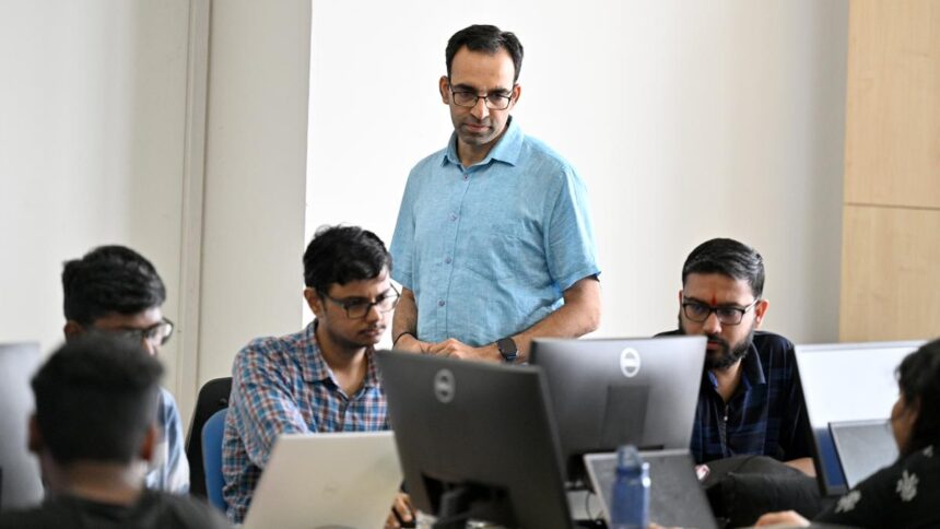
Anuj Grover in contrast the chip manufacturing course of with city capabilities. Similar to the way in which town wants architects, masons, carpenters and plumbers, chipmaking additionally requires semiconductor architects and designers for chips to work, he says. | Picture credit score: Murli Kumar ok
The parallelism of cities will not be an exaggeration. The tip is so refined that the microscope can actually scratch solely the floor. Layers of circuit layers cross particular chips and pack billions of particular person transistors right into a single unit. There’s a purpose why few international locations have a lead in chip manufacturing. This can be a expertise that requires extremely delicate precision devices, even the slightest impurities within the water, and even the precise undetectable variation within the energy that powers the gear, which might smash the yield of manufacturing drives.
Easy accessibility to software program
The federal authorities has bought bulk licenses for the software program suite of main EDA instrument builders as a part of the chips within the Indian Semiconductor Mission Startup (C2S) program. Dozens of universities in India are at present accessing these instruments, and the dashboards maintained by the federal government present that, cumulatively, college students have recorded tens of millions of hours on these instruments.
“We paid 3-4 laks a yr in renewal charges earlier than the C2S program,” stated Nilima Warke, professor on the Institute of Private Engineering. And it was only for instruments from one supplier. Presently, college students and school have free entry to 4 completely different toolsets. This time we’re accessing “skilled bundles” used within the trade fairly than the restricted tutorial ones they’ve used earlier than.
Warke and certainly one of her colleagues designed a 180 nanometer (NM) chip that’s “taped out” at Mohali’s semiconductor lab. The 180 nm chip is comparatively giant – the so-called “legacy” nodes, in comparison with the “frontier” 3-7 nm chips on most superior cellphones – level out that a lot of this coaching was inherently tutorial. A couple of years later, college college students are additionally engaged on frontier-level design. ”
Nonetheless, even when one of these software program is free from handheld sickness, semiconductor design corporations are already profitable. Tessolve, a Bengaluru-based design firm, has been working since 2004, with places of work in 9 cities in India and operations in 10 different international locations. Hero Group acquired a majority stake within the firm in 2016, and Tessolve introduced it had raised $130 million this yr. “Many cities we run are Tier-2,” Tessolve CEO Srini Chinamilli stated in an interview with Zoom in Singapore. “There are lots of people searching for alternatives in locations the place they’ve a extra emotional connection.” In different phrases, it is nearer to dwelling.

Semiconductor die inspections are being carried out in Tessolve Semiconductors in Bengaluru. | Picture credit score: Murali Kumar ok
Chinamilli stated that it labored, and employees have been logged in from giant centres like Hyderabad and Bengaluru, in addition to small cities like Visakhapatnam and Coimbatore.
The hole within the pupil trade
“After Covid, the trade has functioned extra comfortably remotely,” he says. To date, so good. Authorities help is considerably useful and the design area is in place in India. Nonetheless, the experience in Indian chips on the college degree is driving the work of frontiers fairly than US areas. Why, and how will you get there?
“Universities must be proactive and related to the trade, in order that the coaching they’re doing is addressing some actual points within the trade and dealing on what the trade is searching for when it comes to employment potential,” says Chinamilli. Glover couldn’t agree any extra. However there is a rub there. “In India, the trade invests solely 0.4% of its revenue or income in tutorial analysis and improvement,” Glover factors out. Within the US and South Korea, these numbers are 10-15 instances larger. Within the US, academia, which collaborates with trade, isn’t just about graduates prepared for trade. The advantages have additionally grow to be a lot deeper for the trade.
Glover summoned the instance of Andrew Kahng, one other professor at UC San Diego. “And have you learnt why he was the worldwide authority of EDA instruments? Once I was working in his lab in 2002, a cadence engineer visited us and stated, “We anticipate that in three years, we’ll have a reasonably whole lot.
Alumni and PhD college students have a ringside view on the largest problems with chip design, removed from needing coaching, and have entered the trade with one thing to contribute shortly. In the meantime, EDA instrument builders who supported these efforts, together with paying PhD. Pupil scholarships visualize preprints and go head-to-head with rivals from months to yr.
PhD scholarships are less expensive than hiring full-time staff to deal with cutting-edge theoretical questions, however Indian corporations appear unprepared to pay even such prices to advance analysis and improvement. “They’re completely joyful to leap off the specialists and pay for Lakhs even with restricted follow-up,” Grover complained.
One other giant IT firm is asking that they not title substandard charges as a result of they sponsor doctoral levels, he says. A candidate engaged on points straight associated to the corporate. And multinational corporations don’t have any compelling purpose to work with Indian students past the small areas already coated within the nation. “Why French corporations sponsor doctorates in India,” asks Glover.
In response to Glover, India has an even bigger downside with the electronics ecosystem, lamenting the economic base of straightforward elements. “There was a time when Indian corporations have been exporting supercomputers to international locations like Germany and the US,” he says. “Now, even the controllers contained in the ceiling fan are imported.”
Larger issues
Nonetheless, the chip itself will not be essentially the most invaluable a part of the electronics ecosystem. “What do you suppose the iPhone materials invoice is,” he asks, lifting up Teal’s telephone, mentioning the value of all of the elements and their meeting. “It is solely 31% of the general gadget value.”
In response to him, the remainder of the worth is design and mental property. The benefit of chip design is in the end a part of the chip worth, and itself a part of the fabric invoice. To take advantage of the final word worth of those elements, he says, India should grow to be a “product nation” and create what the world truly desires to purchase. And design is a vital a part of that. “Even the button association on this telephone is patented,” he factors out.
The excellent news is that adoption has not waned so far as design and {hardware} testing is anxious. One Bit Pilani alumnus identified that on social media platform X, over 60 college students have been welcomed to placements at Nvidia (‘Bits Pilani nvidia campus’), as if the remainder of the tech trade was caught up within the slowdown.
“Now, it is only a will,” Glover says. “The elements are throughout us.”